Archive for the ‘Homebrew PCBs’ Category
Posted by retromaster on August 22, 2011
-
-
Toner transfer over copper foil
-
-
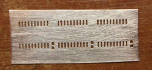
Stencil after etching and cleaning
-

-
Solder paste deposited using the stencil
-

-
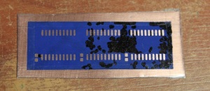
Assembled PCB after reflow
Over the weekend, I decided to try out making a stencil for solder paste from copper foil. I had thought about this previously, but after seeing an instructable on the same idea, I became more confident that it would work.
The process for making a copper stencil is basically the same as making a PCB. The resist image (i.e. paste layer, inverted) is transferred onto the copper foil using any method of your choice. For my tests, I did PnP Blue toner transfer onto 0.2mm-thick copper foil using a laminator. Afterwards, the back side of the foil is covered to prevent etchant from eating away all the copper. I used clear packing tape for this step. The one crucial thing here is to make sure no air bubbles remain in between the tape and the foil. Finally, etching is performed as usual and after cleaning and removal of the tape, one gets a nice looking stencil as shown in the photos above.
One thing to note is that, if one leaves the tape in place, this method can also be used to make simple flex PCBs. This could be quite useful for repair purposes, as well.
Although in my tests the stencil came out pretty well, the reflow (using a hotplate) did not go all that well, as the photos above show the bridges in between some of the legs. This can be due to several reasons: The paste itself wasn’t at very good condition to begin with, more flux may have been needed, the stencil may have been too thick (too much paste), and surely I could have done a better job when depositing the solder paste. Nevertheless, this is not too bad for a first try, and I am confident that I can tweak and improve the process over time for near perfect results for larger PCBs.
Posted in Homebrew PCBs | Tagged: Copper Foil, Flex PCB, Hotplate, PCB, PnP Blue, Reflow, Skillet, Solder Paste, Stencil, Toner Transfer | Leave a Comment »
Posted by retromaster on October 13, 2010
-

-
Cumulus Prototype Board Assembly Progress
Here is a picture of the Cumulus prototype board in its most current state. It is almost fully populated, except for the socket for the 28C EEPROM (I’ve run out of suitable sockets, it seems) and the HCT221 circuitry for MAP signal timing. The CPLD is available through JTAG and the PIC is accessible through ICSP. It took a while to get to this stage, as quite a few things got in the way and others simply went wrong… but now, everything seems to be back on track.
So, what were the problems? First of all, my JTAG Cable decided it won’t work any more… It may have something to do with all the abuse it had to withstand :). Upon building a new one, I got the CPLD connection to work. Very good.
Then I went on to trying the ICSP connection to the 18F46K20, which did not work (to my surprise). So, I spent about a week, debugging on and off, where I checked all the connections, available schematics, etc. The Microchip starter kit schematics had a 8.2V zener diode on the MCLR pin, (my first thought was that was what was missing), but it ultimately turned out to be unnecessary with the PicKit 2, as long as PIC 18F K Series configuration was selected in the software. Finally, I built a couple of very simple boards, basically only with the PIC and ICSP connector on them, just to test the connection to PicKit 2. Those boards worked absolutely fine… Another round of checking, and it turned out that the problem was a fault on the Cumulus prototype board, where the PGD pin had a tiny short to ground. I have no idea how it slipped the first time, but it did. Anyway, now, ICSP is working fine.
So, now I can proceed in two directions. I can finish populating the board, write an Oric test program to the EEPROM (something simple that prints out a text message) and test that the Oric Bus interface is working fine. I can also go on with the UI board, and get the LCD and buttons on it to work, which should be very helpful with the debugging. Hopefully, whichever path I take, things will go a bit more smoothly this time.
Posted in Homebrew PCBs, Projects, Retrocomputing | Tagged: 18F46K20, CPLD, Cumulus, Floppy Emulator, ICSP, JTAG, Microchip, PCB, PIC, PIC18, XC95144XL, Xilinx | Leave a Comment »
Posted by retromaster on August 23, 2010
-

-
A2601 Rev B Homebrew PCB Assembled
-

-
A2601 Rev B NTSC Color Bars Output
I’ve (mostly) finished soldering the new A2601 board. The Xilinx Impact software recognizes the on-board FPGA and Configuration PROM through the parallel port JTAG cable, so I am able to download designs into the FPGA. Just for testing, I’ve uploaded a small design that outputs some NTSC color bars through the composite video port, and it seems to work fine.
It seems some more work needs to be done to get the A2601 FPGA design to work with the new board, though. It has been quite a while since I last worked on this project (judging from the dates on the files, almost three years), and during this time FPGA software (i.e. synthesis, simulation, etc.) has moved on. So I need to remember all the little bits and pieces and fix a few things here and there to make sure that the design works fine in the simulator again (it previously did). Once the design works in the simulator, it should be fine in the FPGA.
Posted in Homebrew PCBs, Projects, Retrocomputing | Tagged: A2601, ATARI 2600, board, FPGA, PCB, Spartan, VHDL, Video, Xilinx | Leave a Comment »
Posted by retromaster on August 16, 2010
-

-
A2601 Rev B Homebrew PCB After Etching Top Side
Having made quite a bit of progress with UFE, I’ve decided it’s time to take a little break from it while I wait and see how recent developments in the manufacturing front pan out (sorry, cannot give details on that yet). So, I am now revisiting a never-before-released project of mine that is almost five years old now.
The project is an ATARI 2600 clone on FPGA, including 6502 and TIA cores in VHDL and dedicated PCB layout, all developed by me. The design fits in a 100K gate Xilinx Spartan 3E, and works quite well in the simulator. The PCB design contains the FPGA, resistor-ladder DACs for video and audio, custom joystick input ports and flash memory for storing ROMs. Few years ago I even built a prototype. It worked well, but unfortunately it did not survive, since my PCB-making techniques were not as advanced back then…
So, what’s new this time around? Basically, a reworking of the PCB layout that fits in a smaller case and contains a single input port for a Genesis/MegaDrive gamepad instead of custom-wired pads. I’ve ended up choosing MegaDrive pads because they are commonly available, very easy to drive and they contain the necessary auxiliary buttons (start/select etc.). I’ve already started manufacturing the board and the photo above shows the work in progress. Hopefully, all will go well and next time I’ll be posting working photos of the board…
Posted in Homebrew PCBs, Projects, Retrocomputing | Tagged: 6502, A2601, ATARI 2600, board, FPGA, Genesis, MegaDrive, PCB, Spartan, TIA, VHDL, Xilinx | Leave a Comment »
Posted by retromaster on June 24, 2010
-
-
UFE Rev A2 PCB Before Assembly
I haven’t posted in a while, but I was not lazy :). I was working on making the PCB for the next UFE hardware revision. I’ve tried a some new things and ran into a few problems in the process, and eventually, came up with the board in the photo.
With this PCB, the soldermask is noticeably stronger than the previous UFE revision, especially on the top side. On the bottom side, the soldermask still lifted in a couple of places. I plan to do some more tests with dummy boards soon and hopefully improve on the process.
One thing that still bugs me here the pitting of copper in large plane areas. Admittedly, this problem is more of a cosmetic nature (as double-sided boards are already limited in terms of signal integrity and speed). I also want to do some further tests to see how this situation can be remedied. Perhaps some Pulsar Green TRF can be useful, or I can even switch back to PnP Blue if I can get it to work with CNC drilled holes.
Posted in Homebrew PCBs, Projects, Retrocomputing | Tagged: Floppy Emulator, Green TRF, PCB, Pebeo Vitrea 160, PnP Blue, soldermask, Toner Transfer, UFE | 2 Comments »
Posted by retromaster on June 10, 2010
-
-
UFE A500 Keyboard Daughterboard Installed
-
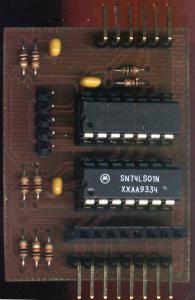
-
UFE A500 Keyboard Daughterboard Top Side
-

-
UFE A500 Keyboard Daughterboard Bottom Side
I’ve fixed the problems in the first A500 keyboard daughterboard I’ve made. Here are some images of the new one, including one that shows how it looks when installed on an A500. At the moment, it works fully with the UFE mainboard. The missing I2C slave writes have been implemented. UFE is fully controllable from the A500 keyboard.
There is one problem, though. The Amiga keyboard protocol requires that the transmitted key event be acknowledged by the Amiga once the full 8-bits of data has been received. If this acknowledgment is not received, the keyboard goes into “lost sync” mode. It stops sending key events, until sync is restored.
Normally, this behaviour poses no problem for UFE, but in some rare cases, some (poorly written) cracks/loaders temporarily assume complete control over the system, causing the acknowledgment to be not sent. For example, the Turrican 3 cracked loader flashes the screen to request the user to swap disks. When in this mode, the loader only checks if the disk is replaced and ignores everything else, including keyboard events. Since the keyboard becomes unusable in this mode, it becomes impossible to activate UFE.
I can think of some solutions to this problem. Probably, one of the more robust ones is to check for the “lost sync” condition in the keyboard daughterboard firmware. If the host fails to respond to the “lost sync” condition after eight 1s have been clocked in, let the keyboard daughterboard acknowledge the last key event. Since the keyboard always retransmits key events that are not acknowledged, no key presses will be lost. Eventually, the host will be able to handle keyboard events properly, and everything should be back to normal.
On a side note, to manufacture this new board, I’ve used a new “drilling technique”. Instead of aligning the toner transfer paper to CNC drilled holes, I did it the other way around. I first did the toner transfer (with holes in pads) and etched the board. Then, using CNC coordinate measurements for four corner pads, I computed the transformation from PCB software coordinate space to etched board CNC coordinate space. This transformation compensates for scaling, translation, rotation and shearing. I’ve written a Python script to do the computation and integrated it within my g-code converter script. As the PCB scans show, the results have been excellent.
I’ll soon update my “Making PCBs” page with all the new experiences I’ve obtained and I’ll release the Python sources for the scripts I use. I am also going to take some scans while I make the new PCB revision for UFE and update the page with those as well. They should be quite an improvement over the poorly lit photos I’ve got there right now.
Posted in Homebrew PCBs, Projects, Retrocomputing | Tagged: Amiga, Floppy Emulator, keyboard, PCB, TFE, UFE | Leave a Comment »
Posted by retromaster on April 26, 2010
-
-
UFE Prototype Assembled
Here is a photo of the UFE prototype, fully-assembled. I am able to program the on-board PIC32 using the PicKit2 programmer. The clock line is connected to the Amiga. Actually, while I was taking this photo, the board was running a tiny test application that alternately blinked the two on-board LEDs. The PIC32 is running at ~75.6Mhz here. The system clock is derived from the 28.375Mhz Amiga system clock, by first dividing the input clock by 6 (to get a ~4.73Mhz clock suitable for the PIC32 PLL) and multiplying it by 16. I am hoping that using the PLL will reduce or eliminate the clock jitter as this was a problem in the earlier TFE+ design, partly due to the relatively long cable over which the clock signal is transmitted. Being able to run the PIC32 at a speed so close to the maximum is very good news, but of course there is no guarantee that problems will not occur with the much more complex setup that will ultimately arise during firmware development.
It is not all good, however. It turns out that my PCB making techniques are still in need of some finetuning. During the soldering process and the cleaning afterwards, the soldermask crackled and popped in several places. I thought it was due to the soldermask not being cured well enough, so it did some tests with a spare, new PCB. It turns out that a thicker layer of paint, plus a higher curing temperature created a much stronger soldermask. During mask removal, the soldermask seems to lose some of its strength, but it works well to cure the board a second time after this step. This step seems to really strengthen the soldermask and that way it is able to withstand soldering and cleaning. I’ll do some more tests to confirm these first findings and finetune the process. Nevertheless, it seems that even in its weak state, a soldermask like this is better than no soldermask at all, since it greatly protects the PCB, especially from the usual trace lifting problems that I frequently experienced previously.
Another issue I encountered with the prototype board was that some of the vias lost connection after the soldermask curing. I am guessing this is due to thermal expansion. I solved the issue by scraping the soldermask above the vias and soldering them on both sides (For hidden vias, I removed the excess solder using a solder wick). This way, a very reliable connection was formed. I’ll soon be updating the page on PCB making with my latest findings.
Posted in Homebrew PCBs, Projects, Retrocomputing | Tagged: Amiga, board, Floppy Emulator, PCB, Pebeo Vitrea 160, PIC32, soldermask, TFE, UFE | Leave a Comment »
Posted by retromaster on April 20, 2010
I’ve just put up a new page here on the processes I use for making PCBs. The page also contains photos of the new UFE prototype PCB and more or less documents the making of it.
Posted in Homebrew PCBs, Projects, Retrocomputing | Tagged: board, PCB, UFE | Leave a Comment »
Posted by retromaster on March 20, 2010
-

-
TFE+ Amiga Version Prototype Solder Side
-

-
TFE+ Amiga Version Prototype Component Side
I finally managed to build the TFE+ Amiga version prototype board. I fully assembled the board but did not install the ICs in their sockets yet.
Apparently, I did a rather sloppy job here. The toner transfer and etching went OK (done using glossy paper instead of the usual PnP Blue). I wanted to apply a soldermask afterwards and that’s where things went wrong. It seems I overcooked the board after applying the glass paint (that’s the reason for the discoloration of parts of the board) and I was not able to remove the masked areas after curing. So I removed the paint layer altogether, and just applied the protective flux layer instead. Well, it’s just a prototype, anyway.
Now, it’s time to get the firmware working on this board…
Posted in Homebrew PCBs, Projects, Retrocomputing | Tagged: board, Floppy Emulator, PCB, Pebeo Vitrea 160, TFE, Toner Transfer | Leave a Comment »
Posted by retromaster on March 12, 2010
It’s been a while since my last post. Most of this time I’ve been trying to deal with the problems I encountered making the TFE+ prototype PCB.
Since I use a CNC to drill the PCB holes, my process is that I get the holes drilled first and then apply the toner transfer. For this to work, it’s imperative that I get the laser printer printout to match the CNC-drilled holes. Previously, I had tested with some smaller boards, and I managed to obtain some fine results. The TFE+ board is quite a bit larger and this is where the problems started. It seemed that a non-linear error kept creeping into the printout and despite trying many different things, I never managed to get a good match.
The printer I’ve been using is a Samsung ML-1610. It’s a fine entry level printer and it has worked well with toner transfer during time I did manual drilling. Once I started having dimensional accuracy problems after the transition to CNC-drilling, I took a micrometer and measured the printout (on plain paper). It seemed that one side of the printout was smaller by almost a millimeter! The error was consistently there in subsequent printouts I took. I have no idea where this error comes from. I am sure that it was not in the source image. It could be a software/firmware error, or it might be that the some parts of the mechanism have worn-out (it’s more than 3 years old now). Or perhaps the printer was never intended to be very accurate (which is fine for a printer in its class).
Deciding that it is time to get a newer (and better) printer, I did some research and came up with the Kyocera Mita FS-1100. It is significantly more expensive than the ML-1610. But it’s built like a tank, it has a much higher speed and 1200dpi resolution, and it seems it may be more economical in the long run. In many ways it reminds me of the older Laserjet line of printers from HP. Last night I did some tests with laser printer transparencies (just to see). The printout from the FS-1100 still needed some scaling, but there was no non-linear error and I managed to get an almost perfect match. Far better than what I got with the ML-1610.
It still remains to be seen whether the FS-1100 output will work fine with toner transfer (e.g. with PnP blue paper). Over the weekend I’ll do some more tests, and if all goes well, I might even have a prototype PCB in my hands next week!
Posted in Homebrew PCBs, Projects | Tagged: Toner Transfer | Leave a Comment »


