-

-
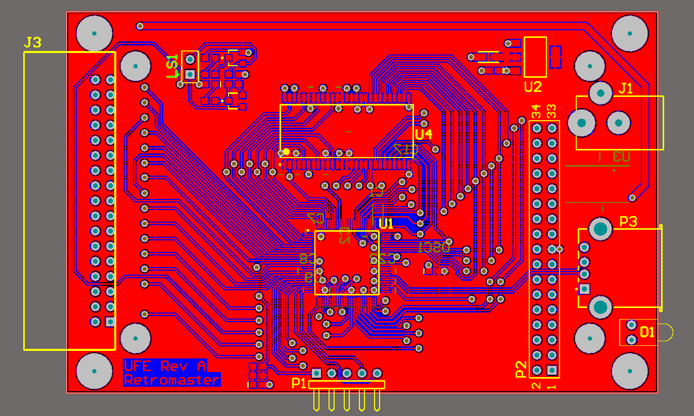
UFE PCB Revision A Top View
For a while now, I’ve been working on UFE, which is the successor to the TFE. It will be considerably more advanced than TFE and (inevitably) more complex and more expensive to manufacture. Some of the planned features are: Full-Speed USB embedded host (enabling use of flash drives as storage instead of SD-MMC card), touch-panel QVGA color LCD user interface (see previous post), read and write support for multiple drives on the same floppy bus, on-board image MFM conversion (using on-board SDRAM).
The picture above shows my first attempt at designing a PCB for the UFE. The main components are a PIC32 microcontroller and a 128Mbit SDRAM chip. The SDRAM is connected directly to the PIC32. The PIC32 has no on-board SDRAM controller, so I plan to emulate it using some software tricks. The same goes for handling of the floppy bus with the SEL lines. If this approach fails, plan B will be to add a flash CPLD to the board to offload some of these tasks to. In this case, I’ll have to redo the design of course, but this first revision will still give me ample opportunity to experiment with the main system components.
The header on the right is for the LCD module daughterboard. The daughterboard will contain the actual socket for the LCD as well as some additional circuitry such as backlight LED drivers. Decoupling these functions from the main board allows me to maintain a degree of independence from the actual LCD module used, and remove some of the associated complexity from the mainboard.
To be honest, I am not entirely sure that I’ll be able to manufacture this board at home. The reason is mainly the 8/6 rules (8 mil trace width, 6 mil clearance) I had to use in the design due to the PIC32, and the high density of the top layer. My previous experiences tell me that 8 mil traces should not be a problem, but I am not sure about the 6 mil clearance.