Retromaster’s Electronics Projects

…related to old computers and other assorted stuff…

Archive for April, 2010

UFE Video Progress

Posted by retromaster on April 29, 2010

I’ve made some progress with the UFE video output implementation. It works in a very similar way to the TFE+, the circuit is almost the same, except that the driver is a 74lvc244 that operates on 3.3V. It uses the SPI module of the PIC32 to shift pixels out and input capture is used to acquire vertical and horizontal sync. Right now, the video data is loaded manually into the SPI registers but I would like to implement DMA as well. Also, the relatively high rate of the peripheral clock gives me lots of room to adjust the horizontal pixel size, which is a nice bonus.

Unfortunately, it does not work perfectly yet as there is quite a bit of flicker (the photo hides most of it but it is quite visible to the naked eye). It looks like whole lines are shifted horizontally by one pixel on a random basis. At first, I suspected the interrupt timing, but the left limit of the video overlay area (also software controlled) shows a straight line with no flicker, so it looks like it must be a timing issue with the SPI module. I’ll investigate further and improve the situation if I can. It is useable in its current state, but since I was able to obtain good quality video from the 8-bit AVRs, I would expect no less from the far more powerful PIC32.

Posted in Projects, Retrocomputing | Leave a Comment »

UFE Prototype Assembled

Posted by retromaster on April 26, 2010

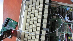
Here is a photo of the UFE prototype, fully-assembled. I am able to program the on-board PIC32 using the PicKit2 programmer. The clock line is connected to the Amiga. Actually, while I was taking this photo, the board was running a tiny test application that alternately blinked the two on-board LEDs. The PIC32 is running at ~75.6Mhz here. The system clock is derived from the 28.375Mhz Amiga system clock, by first dividing the input clock by 6 (to get a ~4.73Mhz clock suitable for the PIC32 PLL) and multiplying it by 16. I am hoping that using the PLL will reduce or eliminate the clock jitter as this was a problem in the earlier TFE+ design, partly due to the relatively long cable over which the clock signal is transmitted. Being able to run the PIC32 at a speed so close to the maximum is very good news, but of course there is no guarantee that problems will not occur with the much more complex setup that will ultimately arise during firmware development.

It is not all good, however. It turns out that my PCB making techniques are still in need of some finetuning. During the soldering process and the cleaning afterwards, the soldermask crackled and popped in several places. I thought it was due to the soldermask not being cured well enough, so it did some tests with a spare, new PCB. It turns out that a thicker layer of paint, plus a higher curing temperature created a much stronger soldermask. During mask removal, the soldermask seems to lose some of its strength, but it works well to cure the board a second time after this step. This step seems to really strengthen the soldermask and that way it is able to withstand soldering and cleaning. I’ll do some more tests to confirm these first findings and finetune the process. Nevertheless, it seems that even in its weak state, a soldermask like this is better than no soldermask at all, since it greatly protects the PCB, especially from the usual trace lifting problems that I frequently experienced previously.

Another issue I encountered with the prototype board was that some of the vias lost connection after the soldermask curing. I am guessing this is due to thermal expansion. I solved the issue by scraping the soldermask above the vias and soldering them on both sides (For hidden vias, I removed the excess solder using a solder wick). This way, a very reliable connection was formed. I’ll soon be updating the page on PCB making with my latest findings.

Posted in Homebrew PCBs, Projects, Retrocomputing | Tagged: , , , , , , , , | Leave a Comment »

New Page on Making PCBs

Posted by retromaster on April 20, 2010

I’ve just put up a new page here on the processes I use for making PCBs. The page also contains photos of the new UFE prototype PCB and more or less documents the making of it.

Posted in Homebrew PCBs, Projects, Retrocomputing | Tagged: , , | Leave a Comment »

New UFE Design Ready

Posted by retromaster on April 19, 2010

As I’ve indicated in my previous post, I’ve been working on a new floppy emulator design, and it’s ready.

The main idea is to implement (hopefully) fool-proof write support by including enough memory to store at least one MFM-decoded floppy image on board. Obviously, your average 40-pin MCU will not be able to access that much external memory, so it was necessary to switch to a more powerful MCU with more pins (in this case, a PIC32). Although static RAM would be simplest to use, they either do not come in the size required or when they do, they are too expensive. So I decided to use SDRAM instead, as there is still a lot of them out there available cheaply in the form of memory modules.

The PIC32 does not have a built-in SDRAM controller, which makes things a little complicated. Luckily, in this project, the external RAM is used like a fast storage area rather than being randomly accessed. So, the plan is to emulate the SDRAM controller in software. It will be accessed quite a bit slower than the usual 100/133Mhz which makes this somewhat easier. In theory, the PIC32 should be able to handle this task, as in comes with a lot of extra computing power, including a built-in DMA controller.

Besides the addition of memory, this new design is a hybrid between the TFE+ design and the older UFE design in terms of features. It features video output for the user interface, just like in the TFE+. The host system’s keyboard will be used to control the emulator, but the keyboard interface is moved to a daughterboard to make the base design host independent. The basic design elements in the original UFE design are in place (PIC32, SDRAM), but SD card is the disk image storage medium instead of a USB flash drive, mainly to reduce complexity of the firmware and simplify PCB layout a bit.

I’ve already started building the PCB for this design and it’s nearing completion. If all goes well, I may soon have another post with the pictures of the actual board.

Posted in Projects, Retrocomputing | Tagged: , , , , , , | Leave a Comment »

Floppy Write Clock Recovery

Posted by retromaster on April 14, 2010

To implement write support for the floppy emulator, the write clock must somehow be recovered from the write data input. The simplest (and probably least robust) way of doing this is in software. When the write enable line becomes active, a “change notice” interrupt on the write data input can be used to detect the first negative-going edge. When triggered, this interrupt would initiate the first SPI receive operation with the proper timing. The rest of the SPI receives would follow, and hopefully there would be little or no jitter on the data (since this is coming from the host). This assumes of course that the host sends data with a perfect 2us interval, which may or may not be the case.

With a little bit of additional circuitry, it is possible to implement more robust clock recovery, which is what I’ve been experimenting with the last few days. I’ve come across a simple circuit based on the 555 timer (CMOS version) used in the Amiga Floppy Reader project. The 555 timer is used to generate the 500khz write data clock, but the write data line is connected to the reset input of the 555 IC. is synchronizes the clock output to the negative-going edges of the write data signal, effectively recovering the clock from the data.

The tiny little board in the photos shows my test implementation of this clock recovery circuit. Early on during my first tests, I realized that there is a minimum width to the reset pulse. This causes the clock pulse to be late. It almost overlaps the positive-going edge of the data signal. Therefore I added a second 555 to delay and enlarge the low pulses of the data signal. That did not work as well as I expected, as the delay introduced by the 555 turned out to be a little too large, as the oscilloscope shot shows.

Another idea that I experimented seems to perform better. Instead of using a 555 for delaying the data signal, a 74hc14 is used to buffer the signal and an RC low pass filter is used to introduce a phase shift. Obviously, a 555 takes up less board space than a 74hc14 and that is why I was experimenting with two 555s instead. A small advantage of the 74hc14 circuit is that there is no need to invert the incoming signal on the MCU side.

As it should be evident from this post, I am already working on a completely new design that will use a PIC32 and on-board memory to fully implement read and write emulation. This is actually a cross between the TFE+ and UFE that I mentioned in one of my previous posts. That is why the test PCB I’ve made uses SMD parts and has a red soldermask, as it was a little exercise for manufacturing the new design.

Posted in Projects, Retrocomputing, Uncategorized | Tagged: , , , , | Leave a Comment »

More on SD Card Write Performance

Posted by retromaster on April 5, 2010

Over the weekend I was able to do some more test on SD card write performance. I’ve tested with two cards: A SanDisk Ultra II (Class 4) and a SanDisk Extreme (Class 10!).

Both cards are SDHC cards (4GB in size). So the first thing was to add SDHC support to the TFE+ firmware. After figuring out some of the quirks of the SD protocol, I was able to get it to work (fortunately, there are many open source examples on the net, which made the process much easier). Both cards were much better performers than the cards I’ve tested previously. However, there are still some unpredictable busy periods during write operations (can sometimes be up to 20ms even for the Class 10 card). They are much less in frequency and size, but they are still there, nevertheless. Due to the reasons explained in my previous post, this dictates having enough memory on board if writes are to be supported on the Amiga.

All that said, the class 10 card was able to support continuous operation to a certain degree and TFE+ was able to write several tracks to the card during a disk copy attempt with XCopy. Unfortunately, the track data was not valid as the SPI clock was not synchronized to the edges of the floppy write data. I may try to implement this synchronization and see if the data is recorded correctly. It also seems that some additional circuitry may be needed here, but I am not sure.

Posted in Projects, Retrocomputing | Tagged: , , | Leave a Comment »

SD Card Write Performance and TFE+

Posted by retromaster on April 2, 2010

Last night I did some tests to determine SD card write performance and its effect on TFE+. The results are not very promising, unfortunately.

It seems that SD cards will always accept incoming data, until some internal buffer is full. Once the buffer is full, there is a busy period of at least 100ms. The size of the buffer and the duration of the busy period varies from card to card. I tried 4 cards of 3 different brands/sizes, and they all exhibit the same behaviour. I am not entirely sure, but I also think some of the cards do not handle very well the situation where a sector is overwritten, and they block until the previous write to the sector is complete.

The trouble is, of course, that since the floppy rotates continously, it is not possible to continuously write to the floppy without hitting the busy period. Most of the time, one can expect that the track will not be continuously overwritten, and the write enable line will become inactive once the track has completed one revolution. Afterwards, the head will be moved to another track and there will be the head settling time. Perhaps, some of the newer, faster (and more expensive) cards will be able to keep up in this case, but it’s difficult to guarantee anything. It may work in some or most cases but probably not in all. It is definitely easier to get this to work in case of a floppy controller with well-defined behaviour, such as the WD1772 in the ST.

Anyway, I think that it makes sense to observe the behaviour of a real floppy drive in write situations and draw conclusions from that. Also, I’d like to measure the performance of some newer cards and see if they’ll be able to keep up. I think the newest of the cards I’ve tried already is at least a year old, and even that one wasn’t a high perfomance card.

Another issue is that, some of the cards do not even guarantee that the data will be written correctly to the SD card. The card specs actually state that there may be write errors and the data written must be verified to see if the write operation must be executed again. This is of course not acceptable in this case, as there is simply not enough time to perform the verification and one of the major advantages of a SD card floppy emulator over a standard floppy drive is (or should be) reliability .

The only proper, guaranteed way of doing this is to include enough memory (in the same order of magnitude as the size of a floppy) on board. All data read through the floppy port would be read from the on-board memory and all data written would go straight to the on-board memory. Then the SD card could be transparently read or written simultaneously in an intelligent manner and this could take as much time as necessary. A led would warn the user to not remove the card if there is data in memory not written to the SD card yet. MFM encoding/decoding could also be performed transparently, as well. Unfortunately, an ATmega644 does not have enough pins or processing power to be able to do this. This is the reason why I had chosen a PIC32 for the UFE project. Now, it seems like a cross between the TFE+ and the UFE may be a good idea.
Posted in Projects, Retrocomputing | Tagged: , , , , , , | Leave a Comment »

Overclocked the TFE+ ATmega644

Posted by retromaster on April 1, 2010

After getting TFE+ floppy read emulation to work, I fixed some bugs and made improvements. Afterwards, I started working on write support. As an optimization that could help with SD card I/O performance, I implemented the multiple block read/write access modes. The idea was to read/write in 2 or 3 sectors at a time instead of just 1. This way, SD card access time overhead is effectively reduced (at least) by half.

The idea worked, but during performance measurements, I noticed that the access time is not the biggest overhead (contrary to what I initially expected). Instead, data transfer time is significantly higher. In my case approximate numbers for read operation would be about 0.5ms to 1ms access time and about 4ms transfer time (for 1024 bytes). This works well for read emulation, but probably not near well enough to get write emulation working.

With some clever optimization of the read routines, I managed to get the transfer time down by about 20-25%. There is even more room for optimization, but the improvement would remain marginal at best. So, I turned to a far more radical solution: Overclocking the ATmega644. This was successfully done in other projects (such as the Uzebox) so I decided to give it a try. I disabled the system clock prescaler and directly used the host ~28Mhz clock instead of dividing it by two.

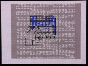
The results are quite good. The transfer time went down to about 1.5ms, making the total SD card read time around 2ms. After quite a bit of testing, there do not seem to be any stability problems, but it may be a good idea to test with other ATmega644s to see how far this goes. A nice side effect of overclocking was that I was able to implement 80 columns text video display as the image above shows.

It is not all quite so rosy, however. I’ve encountered an interesting problem. All the time during testing, I had my oscilloscope’s ground clip attached to the Amiga’s RF shield. With this, TFE+ runs great, but as soon as detach the clip, TFE+ becomes very unstable, and sometimes does not even boot. I do not think it is related to overclocking, as I’ve seen it before. It probably points to a strange grounding problem somewhere, perhaps something to do with the PCB layout. I’ll investigate this problem further.

Posted in Projects, Retrocomputing | Tagged: , , , , , | Leave a Comment »