Making PCBs
I’ve been making double-sided printed circuit boards in my home workshop for quite some time now. This page is an attempt to document the processes I usually follow and experiences I’ve obtained making PCBs.
The common methods of making PCBs at home (e.g. using toner transfer) have been quite well documented throughout the net. My intention here is not to provide a tutorial covering the basics. Instead, I briefly cover my own setup and processes from start to finish and share some of my own experiences as well as elaborate on some usually overlooked topics such as vias and soldermasks. Since I am continuously experimenting and finetuning the processes, I expect to make frequent updates to this page to reflect any progress I may achieve over time.
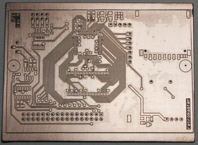
Due to my almost non-existant photography skills and poor setup, most of the photos on this page do not do justice to the actual results. Especially the soldermasked PCB below looks much better than the photo here.
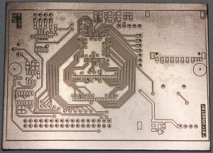
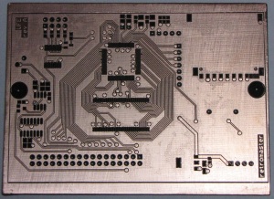
-
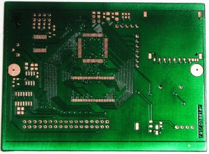
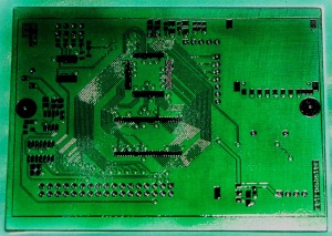
- Homemade Board with 8 mil Tracks, 6 mil Clearance, Vias and Soldermask
Equipment
Laser Printer (Kyocera FS-1100, for toner transfer), CNC Mill/drill (converted Proxxon MF70, for drilling copperclad), Office Laminator (Generic brand, for toner transfer), Light-box (self-made, for pattern aligment), Via press (self-made, for making vias), Airbrush (Proxxon MK240 compressor and additional airbrush, for soldermask application), Toaster Oven (Generic brand, for soldermask curing).
Materials/Supplies
Copperclad board (Phenolic or epoxy fibreglass substrate), Toner transper paper (Glossy/magazine or Press’n Peel Blue), Etchant (Ferric Chloride), Drill bits (Tungsten Carbide), Cleaning supplies (Scotch-brite, Acetone, Paint Thinner), Copper wire (for vias), Soldermask (Pebeo Vitrea 160 Glass Paint).
Process
Layout: Apart from the usual guidelines of PCB design, there are a few basic rules that I generally follow to make sure that I can actually manufacture it. For example, since I am not able to make plated through-holes and vias, I ensure that through-holes can be soldered on both sides if they are to complete an electrical connection. If this is not possible, I either route the board in a different way or I place a mechanical via nearby. So far, I have been able to achieve 8 mil wide traces with 6 mil clearance, but I use wider traces/clearances wherever I can. I also maximize the use of copper pours to save on etchant and to speed up etching.
Drilling: Since I use a CNC to drill the board, drilling comes before the toner transfer, as it is easier to align artwork to drilled holes than the other way around. I fix the copperclad to a piece of MDF using strong double-sided adhesive tape to make sure that the copperclad stays flat during drilling. I’ve written a little Python script that converts .nc drill files to G-code for use on my MF70 CNC.
It is crucial to use sharp tungsten carbide bits to have clean holes with no burrs. I usually use 0.5mm bits for vias and 0.8mm for through-hole components.
-
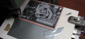
- PCB Drilling with MF70-CNC
-
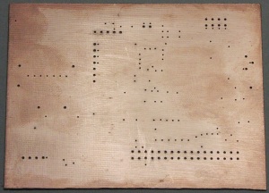
- CNC Drilled Copperclad
Toner transfer: I print the artwork to the transfer paper using my laser printer. Then, I align the artwork to drilled holes on the copperclad using the light-box I’ve made. Finally, I pass the combination through the laminator several times (usually about 8 to 10 times) to perform the actual transfer. A clothes iron may be used for really small boards, but I find that a laminator is a must for accurate, high density transfers for larger boards.
I have found out that, since laser printers usually have poor dimensional accuracy, it is usually necessary to scale the output slightly to have it match properly to the holes. I export gerber files from the design software and I use an excellent little utility called gerber2pdf.py to obtain the scaled artwork. The scaling errors for both axes are usually less than 1% but even such seemingly small errors are enough to cause misalignment. As long as the errors are linear, they are not difficult to compensate for.
I’ve tried two different kinds of paper for transfers: The Press’n Peel Blue and glossy (magazine) paper. Both work well for relatively high density artwork. Here is a comparison of the two, based on my experiences:
- Stability: Compared to magazine paper, deformation of PnP Blue under heat is more irregular. This can make alignment of PnP Blue prinouts to drilled holes is more difficult and less accurate.
- Cleanliness: PnP Blue tends to pull small dust particles which means touch-ups are invariably required after the transfer. This is less of a problem with glossy paper.
- Removal: PnP Blue can be removed right away from the copperclad after the transfer. Glossy paper requires the board to be soaked in water for a while and very careful cleaning afterwards to remove residue.
- Transfer Quality: PnP Blue creates much better copper fills/pours compared to the glossy paper. With PnP Blue, copper fills look completely solid, but in the case of glossy paper, copper fills usually have tiny little pits in them. This can be fixed to a degree by strengthening those areas with resist pen. Thin tracks are fine with both kinds of paper.
- Resolution: I’ve successfully made boards with 8 mil tracks and 6 mil clearance with toner transfer using both kinds of paper.
- Price: Glossy paper wins hands down as there is simply no comparison.
Currently, my primary choice of toner transfer paper is glossy paper, with price and stability being the determining factors.
-
- Toner transfer with Glossy Paper
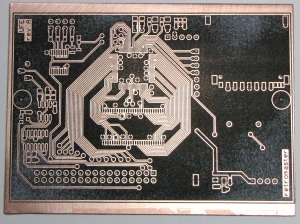
Etching: My etchant of choice is Ferric Chloride. I warm the etchant beforehand and I keep agitating the board until etching is complete. It usually takes around 6-7 minutes. I would like to experiment with other chemistries such as Cupric Chloride, but I have not had the chance yet.
For producing double-sided boards, I usually do toner-transfer and etch one side at a time. I mask the other side using wide clear adhesive tape.
-
- After Etching
Vias: The “right way” of making connections between the top and bottom layers of a double-sided board is by “plated through-holes” (PTH). It is not impossible to do PTH at a home workshop such as mine but it is not easy to obtain the required chemistry and equipment (i.e. electroplating tank). I also doubt that it would be economical in very low volumes.
The simplest way of making a via is by putting a wire in the via hole and soldering both sides. This can work very well, except when you have an SMD board and the need to put vias under an IC arises (this happens almost always). Mechanical vias are a solution that can work well in that case. Special rivets can be used for this purpose, but they are not necessarily cheap.
I built a device that I call a “via press” that can be used to make mechanical vias. I place a small piece of copper wire in the via hole. It needs to be a tight fit so that it won’t slip out of the hole. I trim the ends of the wire so that very little (perhaps less than a millimeter) of it sticks out of the hole in both sides. Then, I place the board in the via press and applying pressure to the board crushes both ends of the copper via and produces a reliable connection between the two sides. More details on the via press can be found in this post.
-
- Mechanical Vias: Full Board View
-
- Mechanical Vias: Closeup
Soldermask: If one is assembling PCBs by hand, a soldermask is probably unnecessary, especially for a prototype. Nevertheless, a soldermask is beneficial for protection of the board, especially from corrosion. Not to mention that it looks much nicer.
The method I use (I first encountered it here) is based on a commonly-available, inexpensive glass paint called Pebeo Vitrea 160. This is a water-based, transparent glass paint that works quite well as a soldermask once it is cured in a domestic oven. It comes in several different colours and in bottle, tube or felt tip marker containers. After application, it requires a drying period of 24 hours before oven curing.
To be able to use this as a soldermask, the solderable areas of the PCB need to be masked from the glass paint. Fortunately, toner transfer also works quite well for this purpose.
The procedure is as follows:
- Toner transfer is applied on the etched board, using the “solder layer” as the pattern. This covers all solderable areas (e.g. IC pads) with toner.
- The whole board is painted with Pebeo Vitrea 160. A 0.5mm nozzle airbrush works best for me. I thin the paint slightly (add 1 part water to 4 parts paint). I haven’t tried paste or markers, those may also work well.
- The board is left to dry. The whole 24 hours may not be required, but I have not experimented enough to specify a minimum.
- The board is cured in the oven. I use an inexpensive toaster oven and an oven thermometer to monitor the oven temperature. I bake the board for 40 minutes and I do not let the temperature to go above 130 C. The paint manufacturer specifies 160 C for curing but I find that sometimes the copperclad stock I use are not able to withstand those temperatures for extended periods of time.
- The areas masked with toner are removed using a combination of paint thinner and acetone, by light rubbing with a sponge. Depending on the thickness of paint, it may take a while for the solvents to take effect.
- After cleaning the solvent remains, the board is ready for soldering.
I do not fully understand the mechanism behind the toner masking of glass paint, but I am guessing that it somehow interferes with the adhesion of the paint on the board surface and this reduces the resistance of the paint against solvents.
-
- Soldermask: After toner transfer
-
- Soldermask: After painting
Remaining Issues
Due to the my laser printer’s poor coverage of black areas, copper fills come out with tiny little pits in them. I am looking for a solution to this problem other than strengthening all affected areas manually with a resist pen.
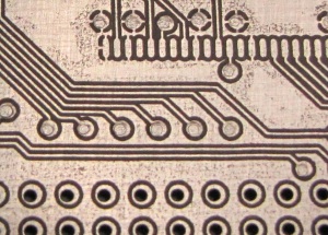
I have not yet exactly determined the scale correction factors to compensate for poor laser printer dimensional accuracy, so there are still minor alignment errors, as is clearly seen from the board photos.
The method I use for making the mechanical vias works quite well, but it is very labor intensive. I am open to exploring less time-consuming alternatives.
The soldermask method needs more testing and experimentation. It is not as strong as a real soldermask. Curing it at higher temperatures (as specified by the manufacturer) may make it stronger, but it could also make mask removal more difficult (if not impossible) and there is a risk of burning the paint and/or the board if the temperature is not controlled well enough. It may also be beneficial to divide the curing step into two: First, a quick cure step before mask removal and a later, longer cure step to really harden the paint. It is also not clear how resistant the glass-paint is against certain fluxes (and solvents used for cleaning those fluxes).

terry said
Hi
Funny how you think you have thought of a unique way of doing something then find some one else is virtually doing the same thing
I was thinking of how to mask the pads and vias before painting with glass paint, and I was going to to try drilling some stiff plastic with holes that are a bit bigger than the pads lay this over the board then scrape some peelable solder mask RAPID code 87-4430 into the holes to cover the pads
once painted the mask should be easy to remove.
Moe said
Best looking DIY PCBs ever, great work. Something tells me you are a perfectionist.
retromaster said
I guess I am 🙂 But definitely not to the point where I can not get things done…
Brian said
Hi,
step 1 that you use the “solder Layer” to protect the solderable pads, Which layer is that, i am new to Eagle and i do not see an option to display a solder layer so i can print, and remask the pads prior to putting the paint on ?
retromaster said
Brian, I am not familiar with Eagle, but I am sure that you should be able to export the solderable areas of the board from any PCB design software in some form (maybe inverted?), since some similar output is needed in professional PCB manufacturing for making soldermasks. Sorry I couldn’t be of more help, someone who knows Eagle well should be able to answer your question.
Chris Phoenix said
Thanks for this site. I like the mechanical vias!
I found this Youtube video that features a UV-curable solder-mask which looks perhaps simpler than your paint method.
I discovered today a way to cut 0.5mm pitch solder paste stencil with a laser cutter. If you just cut the mylar, it will melt the tiny strips between the pads. But if you put the plastic on a wet piece of paper, the laser still goes through, but it does not melt beyond the beam, and the edges are very clean.
I used a thick scrap piece of acrylic as a base, put a piece of ordinary laser printer paper on it, poured on a bit of water, put the 2 mil mylar on that, and then smoothed it out and blotted up the excess water. You want the water to get on both sides of the paper and soak it through.
On an Epilog (45 W? I’m not sure), a vector speed of 50, power of 10, and frequency of 5000 was more than enough to cut through the mylar… but not melt it. It works on both 2mil and 6mil. I shrank all the pads by 6 mil, but I’m not sure you have to… it worked well enough that I did hardly any tuning of the process.
If anyone reading this is near Menlo Park, leave a comment here; I hang out at TechShop.
retromaster said
That UV-curable soldermask is the real deal of course, and it is probably stronger than the glass paint. The problem is that I already had a toner transfer setup and I wanted to make optimal use of that. There is also the problem of actually obtaining the UV-curable soldermask, too.
Mate Lampert said
Hi retromaster!
First I would like to congratulate to you for the great work, and I am truly amazed of the quality of your DIY PCB. That is something I have never seen amongst the DIY PCBs.
I have two questions:
The first is: Could you tell me exactlyy what is the paint thinner that you are using?
The second is about the through hole vias. I saw another good DIY method, which used vacuum suction and radiator repair fluid, which sticked to the holes after the vacuum sucked the material through it and it remained there and it became solid immediatelly. The website is here: http://www.colinmackenzie.net/electronics/14-pcb/25-thru-hole-plating-diy-printed-circuit-boards
Did you try out something like this?
retromaster said
Hi Mate Lampert,
Thank you very much for your kind words, I am really glad you like my PCB work. My answers to your questions:
1) The label on the bottle just says “synthetic paint thinner”, without any more information. It is the standart kind of paint thinner sold where I live.
2) I have seen the method you’ve described before, but not tried it yet. It sounds very promising, but probably not perfect yet. It looks like the success of that method depends on finding an inexpensive conductive liquid that can form (very) low impedance vias when dried. I might try it one day, if I get around to building a vacuum table.
ed said
Hello your pcbs look fantastic. I am currently looking up the toner transfer method because I want to make some new pcbs with new fine pitch smds etc. Another guy at a webpage I looked at, he also had the problem of pitted copper fills, and thought that it was a characteristic of the laser printer driver. Anyway he tried using a crosshatch pattern to the copper fills, instead of solid, and this got rid of the problem – removed the pits. Also crosshatching still looks professional too. Great work, thank you.
Steven said
Thanks for the well-written article. I’m getting started with this whole toner-transfer thing, and the more I learn about other people’s successes, the better.
re: “Due to the my laser printer’s poor coverage of black areas, copper fills come out with tiny little pits in them.”, are you familiar with this product: http://www.pcbfx.com/main_site/pages/start_here/overview.html ? They claim that their film solves that problem by sticking to the toner and filling in the gaps a bit. I have purchased one of their kits, but haven’t tried it yet.
retromaster said
@Steven: I am familiar with that product, in fact, just like you, I bought some of their green film, but I haven’t tried it yet. Partly because I do have some stock of PnP Blue still remaining, which I use whenever the pits bother me too much.
Rod said
Hi Retromaster,
Thanks for these excelent tips XD
I’m using curable UV paint for the soldermask, but i have a problem.
After painting the pcb with UV paint, i put a transparent film to spread the paint, and over that i put the soldermask print (the pads only), and finally a glass. Put it ono uv light for 15 min. And then, when I remove the transparent film over the paint, some paint goes with these film…
Do you have any idea how could I avoid these problem ??
Thanks
(sorry for my english, i’m from Chile)
Rod
retromaster said
Rod,
No need to apologize for your English.
I am afraid I have no experience with curable UV soldermask paints. But surely there are things you could try: Increase uv light exposure time, use a different type of transparent film, maybe clean the pcb better so that the paint adheres better? Let us know what results you have.
Btw, what kind of UV paint are you using? Where did you get it?
-RM
bearmos said
Nice looking PCB’s, Retromaster! I’ve also had issues with pitting using glossy paper – although much worse becase I’m using an old laser printed with a worn-out fuser. At any rate, PTH’s aren’t quite as bad as they might seem initially. I’m in the middle of writing up a process adapted from thinktink.com – currently I’m aiming at milling the traces, instead of chemically etching, since it doesn’t require an additional tin plating before etching.
I’ve got some articles detailing setting up the plating tank and solution, if you’re interested in taking a look. Again, it’ll be a little bit more complicated if your’e chemically etching, because you need to plate the through holes before etching, then apply a resist that will cover the inside of the plated holes (otherwise the copper in the PTH’s will etch away) – from what I understand this requires another process tank (tin plating i believe).
retromaster said
Bearmos,
I’d definitely be interested in having a look at those articles you mention. IMO, homebrew PTH is very important, not just for making pretty PCBs, but because it is the most crucial step to making quality multi-layer boards.
On account of the interaction of PTH and chemical etching, does the method you’re going for have a hole-wall activation step?
-RM
zika said
Just one addition, I really think it is better the drill only the mount holes pre etching. So you use mount holes to alling top/bottom foils. When you drill all holes pre etching the etchant always kill your copper on the edges of the holes
retromaster said
Zika, that hasn’t been my experience, but I take extra care with smoothing out the copperclad and removing the burrs near the holes. I also strengthen the resist with a pen around the holes if I see that the PnP did not adhere well to the sides of a hole.
Albert Kurucz (@albert_kurucz) said
Nice results, and probably more fun, but is the home brew more economic?
retromaster said
Probably not more economical, especially if you factor in the time spent doing all these steps and redoing the occasional mistakes. And even at prototype quantities, one usually gets several boards from professional board houses. From a material cost only viewpoint, homebrew is definitely more economic, though.
Apart from the fun aspect, all this stuff is very useful for testing new circuit ideas or new components, as those are usually one-of-a-kind, small projects. Sending those out to a board house would take too long and would be too expensive.
One thing that could potentially change the economics picture is if someone comes up with a practical way of homebrewing multi-layer boards. Multi-layer PCB prototypes are quite a bit more expensive and this makes it costly to try out more advanced parts in homebrew electronics projects.
Steve Reberger said
Thanks for some great ideas on vias and solder masking.
I use the toner transfer method but instead of using a laminator, I have made a small press out of 2 pieces of 10mm thick aluminuim bolted together. I place the board and pattern in the press along with a piece of cork. I then clamp the whole lot together and place in an oven at 180 degress celcius for 10 minutes. I find this give me quite consistant results.
HopeThisHelps said
Hi
Not sure if you have tried the following yet, it works well for me and is very cheap:
I use contact paper instead of magazine or PnP to print my circuits onto for toner transfer method. The trick is to discard (maybe use it for something else – lol) the plastic that the contact paper was actually made for (It will mess your laser printer when it melts so please don’t use that in your laser printer) and use the paper it is stuck to. Using Pritt or some other glue (I first used masking tape to hold it in place) one glues the paper side to an A4 sheet where the PCB will be printed. Ensuring the plastic/glossy side is printed on. Then iron this to your copper board and let it cool, it just peels off similar to PnP as soon as it is cooled (I place it under running water to cool it quicker).
The contact paper I refer to is seen in the following link: http://www.squidoo.com/cover-a-book-with-contact-paper
(I had to find a better material than magazine paper and a cheaper, more accessible, way than PnP, South Africa doesn’t have much to offer in DIY PCB making. haha)
Hope this helps make somebody’s DIY easier.