-
- Toner transfer over copper foil

-
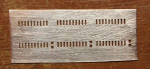
- Stencil after etching and cleaning

-

- Solder paste deposited using the stencil

-

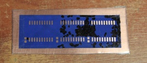
- Assembled PCB after reflow

Over the weekend, I decided to try out making a stencil for solder paste from copper foil. I had thought about this previously, but after seeing an instructable on the same idea, I became more confident that it would work.
The process for making a copper stencil is basically the same as making a PCB. The resist image (i.e. paste layer, inverted) is transferred onto the copper foil using any method of your choice. For my tests, I did PnP Blue toner transfer onto 0.2mm-thick copper foil using a laminator. Afterwards, the back side of the foil is covered to prevent etchant from eating away all the copper. I used clear packing tape for this step. The one crucial thing here is to make sure no air bubbles remain in between the tape and the foil. Finally, etching is performed as usual and after cleaning and removal of the tape, one gets a nice looking stencil as shown in the photos above.
One thing to note is that, if one leaves the tape in place, this method can also be used to make simple flex PCBs. This could be quite useful for repair purposes, as well.
Although in my tests the stencil came out pretty well, the reflow (using a hotplate) did not go all that well, as the photos above show the bridges in between some of the legs. This can be due to several reasons: The paste itself wasn’t at very good condition to begin with, more flux may have been needed, the stencil may have been too thick (too much paste), and surely I could have done a better job when depositing the solder paste. Nevertheless, this is not too bad for a first try, and I am confident that I can tweak and improve the process over time for near perfect results for larger PCBs.


