A2601
A2601 is an FPGA-based clone of the legendary ATARI 2600 video console, developed completely by myself, including VHDL code and a custom PCB.
-
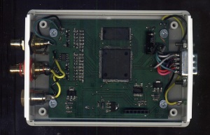
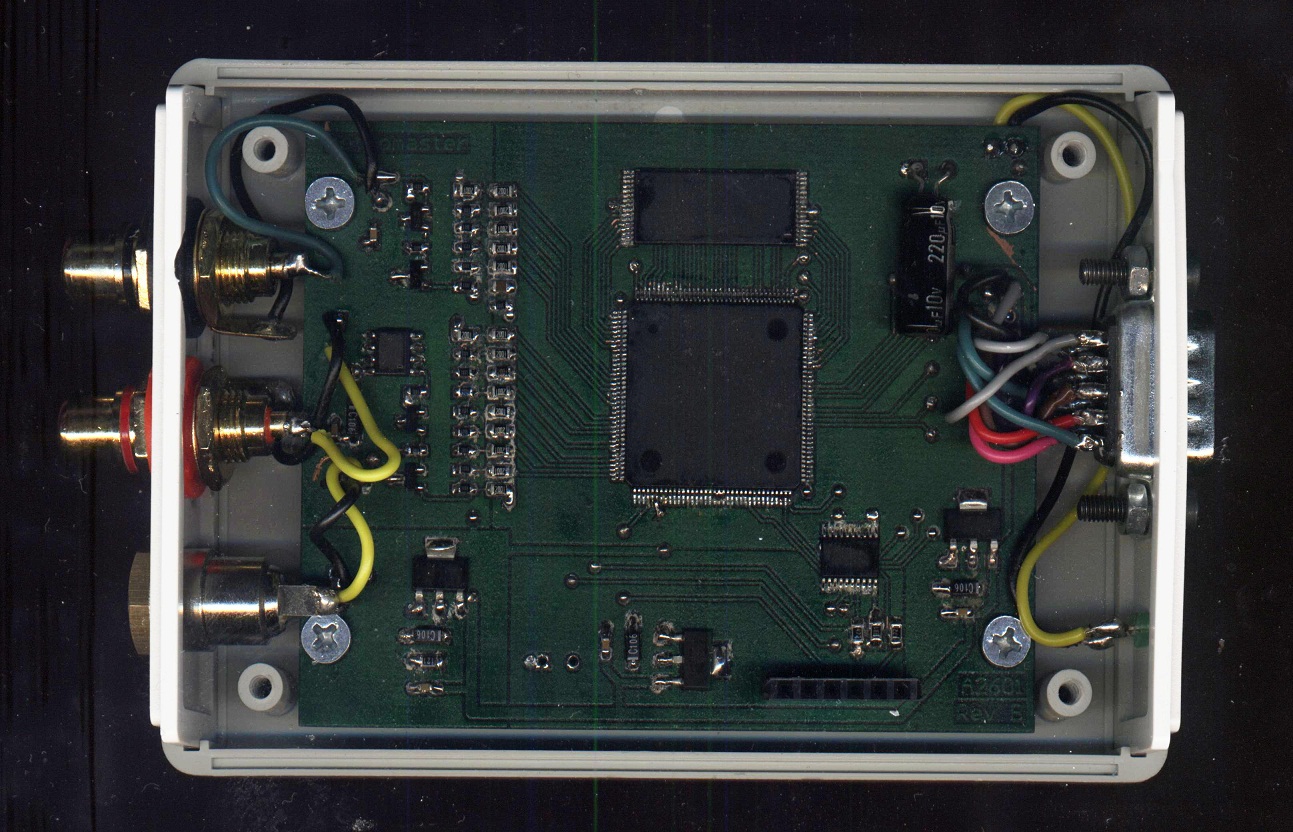
- A2601 Rev B Homebrew PCB Installed in Plastic Case
-
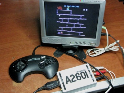
- A2601 Complete View Running Donkey Kong

-
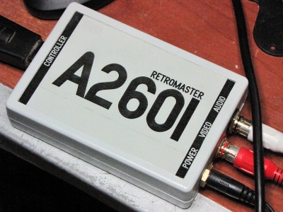
- A2601 Case Closeup

-

- A2601 Running Pitfall

-

- A2601 Running Keystone Kapers

-
- A2601 Running Track and Field

-
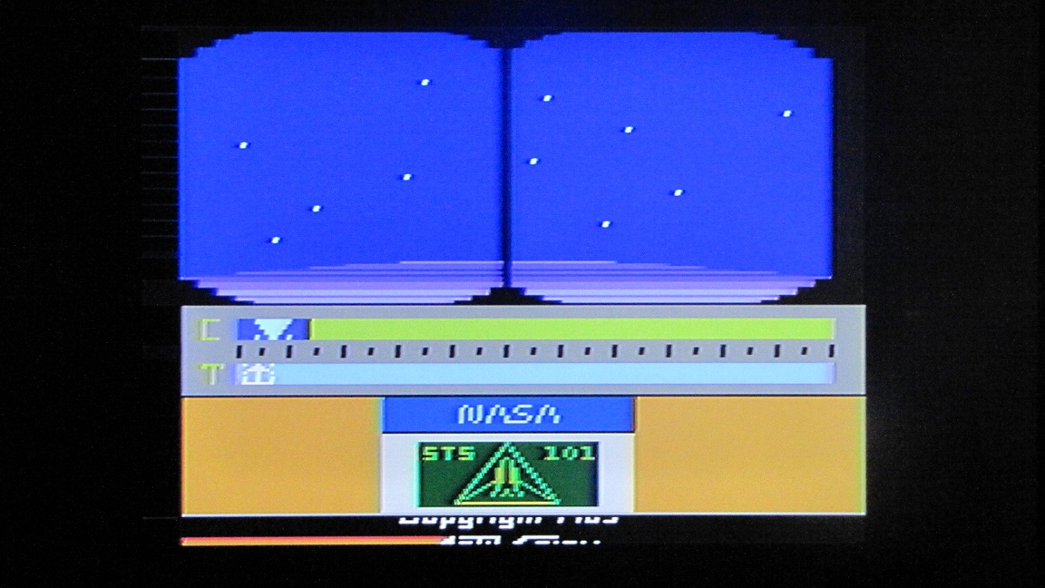
- A2601 Running Space Shuttle
-
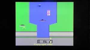
- A2601 Running River Raid

-

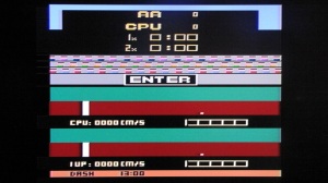
- A2601 Running Pressure Cooker

Features
- Faithful FPGA implementation of the 6502 CPU and TIA (Television Interface Adapter) custom chip.
- Composite Video (currently NTSC only) and Audio output.
- DB9 connector for a MegaDrive/Genesis joypad.
- On-board 512Kb Flash memory for storing cartridge roms.
- Support for most bankswitching schemes used by original game cartridges.
- Design fits in a 100K-gate Spartan-3E FPGA.
- Custom PCB dimensions: 3.25″ by 2.5″.
- Complete VHDL source code available under GPL.
Videos
All game videos and screenshots featured on this page have been shot using a digital camera pointed towards an LCD TV connected to A2601.
How to use
A2601 Rev B PCB contains the following connectors:
- Composite Video (Standard Phono Connector)
- Audio (Standard Phono Connector)
- Power (9V, positive inside)
- Joypad (DB9, MegaDrive/Genesis)
The B button on the joypad acts as the fire button. The Start button works as the “Game Reset” button. When the A button down is held down, the direction buttons function as the switches on the console main unit (i.e. “Difficulty”, “Select”, etc.). Holding the C button down and pressing left or right moves to the previous or the next game on the flash memory, respectively.
Technical Information
-

- A2601 Rev B Schematics Sheet 1

-
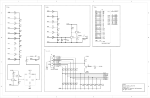
- A2601 Rev B Schematics Sheet 2

-

- A2601 Rev B Schematics Sheet 3

A2601 Rev B Board contains a TQFP 144-pin Spartan-3E FPGA, an XCF01 Configuration PROM, a 29W040B Flash Memory. The on-board JTAG connector allows programming of both the FPGA and the Configuration PROM. There are 4 linear voltage regulators on the board, supplying 5V, 3.3V, 2.5V and 1.2V. A 14.318 Mhz oscillator supplies the main clock signal for the FPGA.
The video circuitry consists of an 8-bit R-2R resistor ladder DAC with a FMS6141 active SDTV video filter output stage. Similarly, the audio circuity is a 5-bit R-2R resistor ladder DAC plus a transistor buffer output stage.
The joypad port is powered through the 5V voltage regulator on board. Resistor voltage-divider circuitry is used to translate joypad output levels to FPGA-safe levels. A transistor buffer is used to drive the SEL line on the joypad side.
To program the 29W040B flash on-board, a specialized FPGA design is used to read commands and data from the Xilinx JTAG port (see the Flash directory in the source code archive). A Python script called bin2xsvf.py is provided to convert binary files to .xsvf files suitable for use with Xilinx Impact software to program the flash memory in conjuction with the specialized design.
The board draws about 85ma of current from the 9V power input (power LED excluded).
VHDL source code provided includes implementation of the 6502(7) CPU, the TIA, the 6532 RIOT, additional audio/video/joypad circuitry and bankswitching schemes plus additional RAM used by some game cartridges. Test benches are supplied for all main components (although they may be slightly out of date).
The 6502 core has been developed from scratch for this project by myself. It contains hand-crafted finite state machine and controls that implement all documented 6502 opcodes. It synthesizes quickly and has good performance in the simulator. The 6502 core is available under GPL just like the rest of the A2601 source code.
The TIA implementation digitally synthesizes NTSC composite video signal via a lookup table that contains a sequence of values that signifies a sine wave at correct phase for each one of the 16 chrominance values selectable in the TIA. A Xilinx DCM multiplies the input clock by four to improve the temporal resolution of the signal. An alternative would be to use a sine lookup table stored in FPGA built-in memory to synthesize the signal. With an improved DAC, this method could enable synthesis of PAL and NTSC signals from a common clock source.
You should be able to synthesize the A2601 in Xilinx ISE without any major problems. Two top level entities are provided: One reads cartridge ROM data from on-board flash memory, the other stores the data in the FPGA built-in SRAM. It is also possible to run A2601 sources in a VHDL simulator. Some helper utilities and a test bench are provided for this purpose in the util directory.
Download
A2601 Release 0.1.0 (Includes VHDL sources and Python script utilities)
Limitations (Future Work)
- PAL video output not supported.
- Starpath cassette loader not supported.
- Undocumented 6502 instructions are not implemented.
- Cosmic Ark starfield effect does not work at the moment.
Background
Most of the work on the FPGA side of A2601 was completed in about three months by 2006, at which point the A2601 was running fine in the simulator. In the following weeks, I first designed and built a generic Spartan-3E FPGA board and a couple of addons for it that contained video and audio output circuitry. Once I got the A2601 to work on this board, I went on to design and build the Rev A board with on-board flash memory. This board was somewhat larger than the current Rev B board as it was designed to fit into a larger plastic case, despite containing a smaller VQFP 100-pin Spartan-3E. It worked quite well, but unfortunately it did not survive, since my PCB making techniques were not as good back then. Recently, I decided to revisit this project and decided to redo the board layout and switch to a MegaDrive/Genesis joypad port, and the Rev B board documented on this page is the result.
Disclaimer
This information here is provided AS IS without any express or implied warranties. While every effort has been taken to ensure the accuracy of the information contained in this text, the author assumes no responsibility for errors or omissions, or for damages resulting from the use of the information contained herein. I will not be held responsible for any damages or costs which might occur as a result of anything related to projects described or referred to on this page. You are not allowed to use information contained in these pages for commercial purposes without my written authorization.

Atari 2600 recreated in an FPGA - Hack a Day said
[…] [Retromaster's] field programmable gate array implementation of an Atari 2600. The processor and video chip have both been built in the 100,000 gate Spartan-3E FPGA, with […]
A2601, an Atari 2600 in an FPGA « Executing Gummiworms said
[…] army stores. I do use Stella alot but it would be nice to have the real hardware or failing that Retromaster's A2601 would be nice. Filed under: Retro Leave a comment Comments (0) Trackbacks (0) ( subscribe […]
Thomas Jentzsch said
Very cool!
But why no illegal opcodes? Lots of modern homebrew require them and all the old Atari consoles support them too.
retromaster said
Initially, I wanted to make sure that the whole thing would fit in the smallest Spartan 3E available, so I gave them low priority. Actually the most useful illegal opcodes could be now added without using up a lot of additional FPGA real estate. Just did not have the chance to implement them yet, that’s all… I do not have anything personal against illegal opcodes 😛
Thomas Jentzsch said
I suppose DCP, LAX, SAX and 2/3 bytes NOPs are the most used ones.
batari said
SBX is also very useful, and IMO nearly as important as the ones Thomas pointed out. Also, the second controller port would be nice.
Darcio said
Man, you have done it! Congratz, now 2600 will live for eternity.
Matheus Gonçalves said
Hi,
I wrote an article about your project, on Geek Online, from Brazil.
You can read in portuguese or translate: http://toad.geek.com.br/posts/13841-faca-seu-atari-2600-em-casa
Thank you.
Matheus
hackaholicballa » Blog Archive » Atari 2600 recreated in an FPGA said
[…] [Retromaster's] field programmable gate array implementation of an Atari 2600. The processor and video chip have both been built in the 100,000 gate Spartan-3E FPGA, with […]
BastetFurry said
This rocks, gona tease a friend of mine to convert that to DE-1 and maybe to work with original carts. 🙂
Bruce said
What a cool project!
Electronics-Lab.com Blog » Blog Archive » A2601: FPGA-based clone of the ATARI 2600 said
[…] FPGA-based clone of the ATARI 2600 – [Link] Tags: A2601, ATARI 2600, FPGA, VHDL, video Filed in Miscellaneous | 1 views No Comments […]
Chris Zeh said
That is awesome!! Good work!!
Papilio Arcade kit | WISH (Alpha) said
[…] Atari 2600 on FPGA – Awesome! A full Atari 2600 on an FPGA, this design actually includes a hardware design with it but it is not clear if the author is interested in manufacturing this hardware. The Papilio One is readily available and offers easy expandability. […]
FPGA y el sorprendente poder del hardware reconfigurable en ALT1040 (Curiosidades) said
[…] clásicos como Pong y Crush Roller. Otros han implementado sus propias consolas basadas en FPGA.Atari 2600Un solo FPGA fue suficiente para reconstruir el viejo Atari 2600. Permite audio, vídeo y hasta un […]
Wstęp do programowania Atari 2600 « OSblog.pl Internet, Social Media, Hardware & Software said
[…] 2600 to konsola starego typu, dlatego posiada wiele elementów, które udało się w obecnych czasach zamknąć w jednym chipie. Wystarczy porównać oryginał z nową konstrukcją […]
Matt Weatherly said
Do you have the eagle files available for this project?
I was also wondering if you thought of adding an actual cartridge port instead of the onboard rom? or would it be possible with this device?
Could you also use the original Atari control with this device?
If not I would still be interested in your eagle files?
I currently used the schematics for the original Atari 2600 and I am almost done finalizing my compact version of that. I also plan to make my own original Atari joysticks.
Thanks,
Matt Weatherly
retromaster said
The eagle files are not available, but I can release the gerber files if there’s interest. You won’t be able to edit those, though.
Adding a cartridge port to this design is not a big deal, except that some voltage-level conversion circuitry would be needed. The FPGA uses 3.3V for its IOs whereas the cartridge has 5V signals.
Of course you could use the original Atari controllers with this device (since they are compatible with the Genesis/MGD controllers), but then you would lose the buttons located on the console (Game Select, Game Reset, TV Type) and the ROM game switching functionality. The extra buttons on the Genesis/MGD controllers are used for those.
Matt Weatherly said
I would be interested in the Gerber files.
the power issue would be an easy fix, however is there any documentation that tells me when pins go to where when I add the slot? I have the pin outs for the carts but what pins would they goto on the FPGA?
As far as the game select, game reset, and TV type I am sure I can improvise something(add buttons to the box). My goal is to use ICs that are still available and still manufactured to make an Atari that takes the original carts.
Thanks,
Matt
(if you prefer you can email me at matt.weatherly@gmail.com)
retromaster said
Did you have a look at the schematics? You should be able to find all the pinout information there.
Are you sure that the power issue would be easy to fix? It’s not just the power supply lines. The FPGA is not able to drive the address lines higher than 3.3V, which may not be high enough. The cart ROM will drive the data lines up to 5V, which is definitely too high for the FPGA, so at least voltage divider circuitry, or ideally a buffer will be required.
Matt Weatherly said
I am glad you said something I was thinking I would be able to just convert the power to 5v for the power didn’t think about the returning power,
so I will have to look at the voltage divider or what to do about a buffer.
So I am guessing A0-A12 and D1-D8 just match up to the FPGA labels?
Thanks for the info, if your interested Ill post my modification when I get them done.
Matt
Matt Weatherly said
Ok, a few more questions, and if I am driving you nuts I can stop asking.
First questions I wanted to add S-video, Composite, and RF as well as the RCA that is already there. However I can find the Video Filter Driver, but they all are asking for more inputs that then current one does. Any suggestions on adding these ports? A reference page would be great….been googling all day.
Second, If I add the cartage slot do I still need to add the Flash memory?
Third, more info then anything I found some buffer ICs that will convert 5v signal to the 3.3v
Thanks again,
Matt
retromaster said
Adding RF is probably just a matter of adding an RF modulator module, but S-Video may be problematic. That’s because S-Video would require two independent analog signals (chroma and luma) but there is only one DAC in the current design.
You can remove the flash memory if you add the cartridge slot.
Matt Weatherly said
Well for now I am just adding the s-video and see how that works, just had to add a cap.
Ok, I am almost done, I have moved the Start and select buttons to the case.
I would like to add a second gamepad port do you know if this design supports that? and if so what pins?
I am looking forward to getting this board ordered and seeing how it turns out.
Thanks again,
Matt
leapingcarpet said
yeah. needless to say – very cool. and I want one 😉
enthusi said
are you going to ‘finish’ it? as in adding illegal opcodes, pal etc?
VERY nice project.
retromaster said
Thanks… Though, I am afraid I do not have much time to work on this project any more, so it’s doubtful that I’ll ever get to implement the missing pieces… 😦
gadgetfactory said
Hello Retromaster,
Love this project, I made some OpenSource FPGA hardware over at http://arcade.gadgetfactory.net. We are currently working on converting the NTSC output from the A2601 project to VGA so it will run on the Papilio Arcade. I just wanted to drop by and let you know about our attempts. 🙂 We are talking about it in the forum right now. http://www.gadgetfactory.net/gadgetforum/index.php?topic=395.0
Thanks,
Jack.